Ohio State opens $20 million semiconductor facility
The Microelectronics Innovation and Technology Cluster aims to bridge the gap between university research and commercial manufacturing for defense and industry partners.
By Tessa Cooper ·
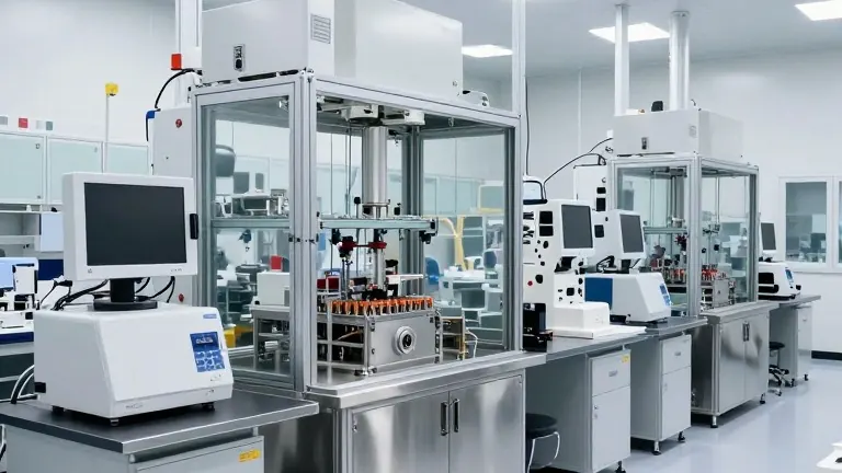
University students and researchers in Columbus, Ohio, gained access to new cleanroom facilities and industrial-grade equipment on Oct. 20. The expansion of the Microelectronics Innovation and Technology Cluster, or MITEC, represents an investment of more than $20 million in semiconductor infrastructure. This development allows local students to work with manufacturing processes that mirror commercial production rather than just academic demonstrations.
The facility connects existing resources at the Nanotech West Lab and the Semiconductor Epitaxy and Analysis Laboratory. Steven Ringel, a Distinguished University Professor and senior associate vice president for research at Ohio State, leads the cluster. He stated that the goal is to support device development for both defense and commercial technology transitions. The integrated environment is designed for rapid prototyping and collaborative work with industry partners.
Funding for the project came from two main sources. Approximately $16 million was secured through the Midwest Microelectronics Consortium, known as MMEC. The remaining roughly $4.5 million came from a collaborative infrastructure investment by Ohio State and the Ohio Department of Higher Education. These funds paid for major equipment additions and facility upgrades. The upgrades expand the university's capacity to help partners evaluate and prepare advanced semiconductor technologies for manufacturing.
MMEC is a regional innovation hub designated by the Department of War. Matt Casto, the CEO of MMEC, described Ohio State as a strategic partner aligned with the mission to strengthen the domestic microelectronics supply chain. Casto noted that the cluster brings together expertise and facilities to accelerate the development of critical technologies. He emphasized that expanding access to these capabilities helps bridge the gap between research and real-world applications.
John M. Horack, vice president for research at Ohio State, highlighted the institution's land-grant mission during the ribbon-cutting ceremony. He explained that the university is committed to moving knowledge beyond the laboratory to translate research into solutions that strengthen communities. Horack noted that while demonstrating a concept in a lab is one thing, achieving it at scale is another. The new infrastructure addresses this scale requirement by using wafer sizes and processes compatible with industrial manufacturing.
The expansion supports workforce development through hands-on training initiatives. MMEC-sponsored fellowships currently provide undergraduate and graduate students with experience in the Nanotech West Lab cleanroom. Students receive training from experienced staff while working on new technologies. This experiential learning component aims to prepare a domestic workforce for the semiconductor industry.
Students in the program work with specific material types. They handle wide bandgap semiconductors used in high-power and high-speed electronics. They also work with narrow bandgap semiconductors required for infrared sensing. By operating at a scale closer to commercial production, the facility reduces the time needed to move new technologies from the laboratory into manufacturing.
The cluster operates under the administration of Ohio State's Institute for Materials and Manufacturing Research. It enhances existing facilities for semiconductor processing, device prototyping, and testing. The facility is now fully operational and available for collaborative technology development. Industry partners and university researchers can utilize the integrated environment for their projects.
More Business · Consumer Alerts · Report a business · Got a Story?